semiconductor manufacturing processes with a 180 nm MOSFET technology node
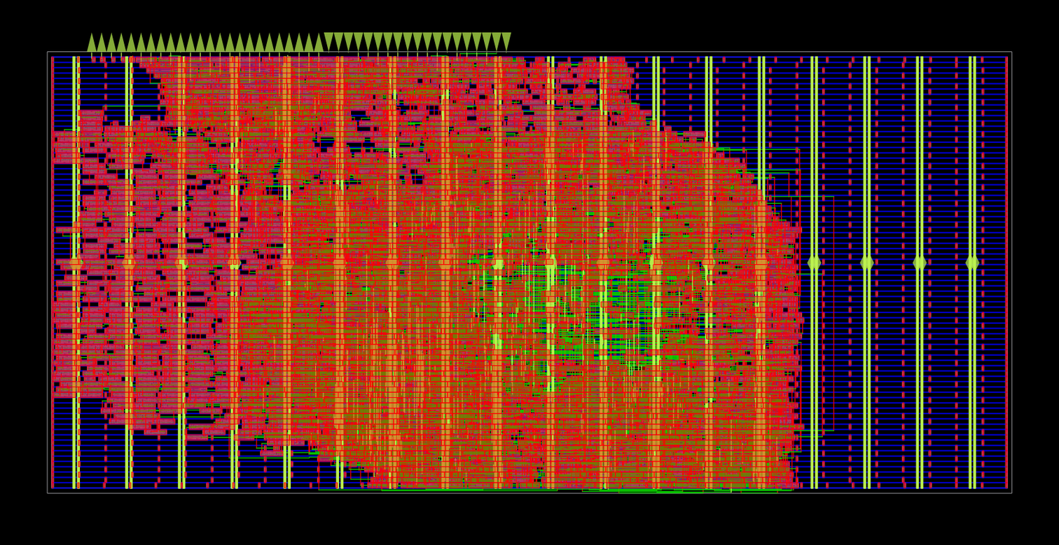
Designing the world's first open source Ethernet switch ASIC. An unmanaged cut-through 3-port 100Mbps switch fabbed on Global Foundries 180 nm.
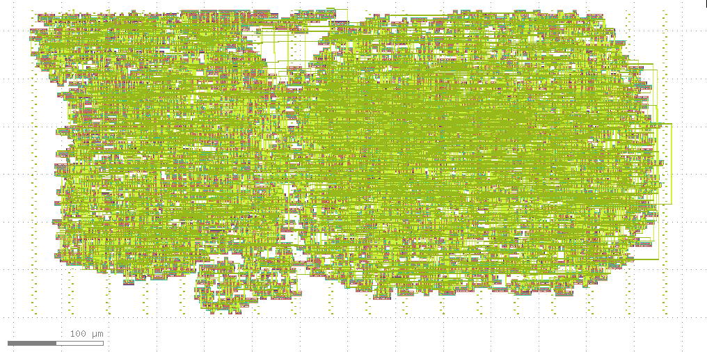
Broadcasting over Ethernet until the heat death of the universe with a custom ASIC, or yet another terrible idea, this time inspired by reddit.
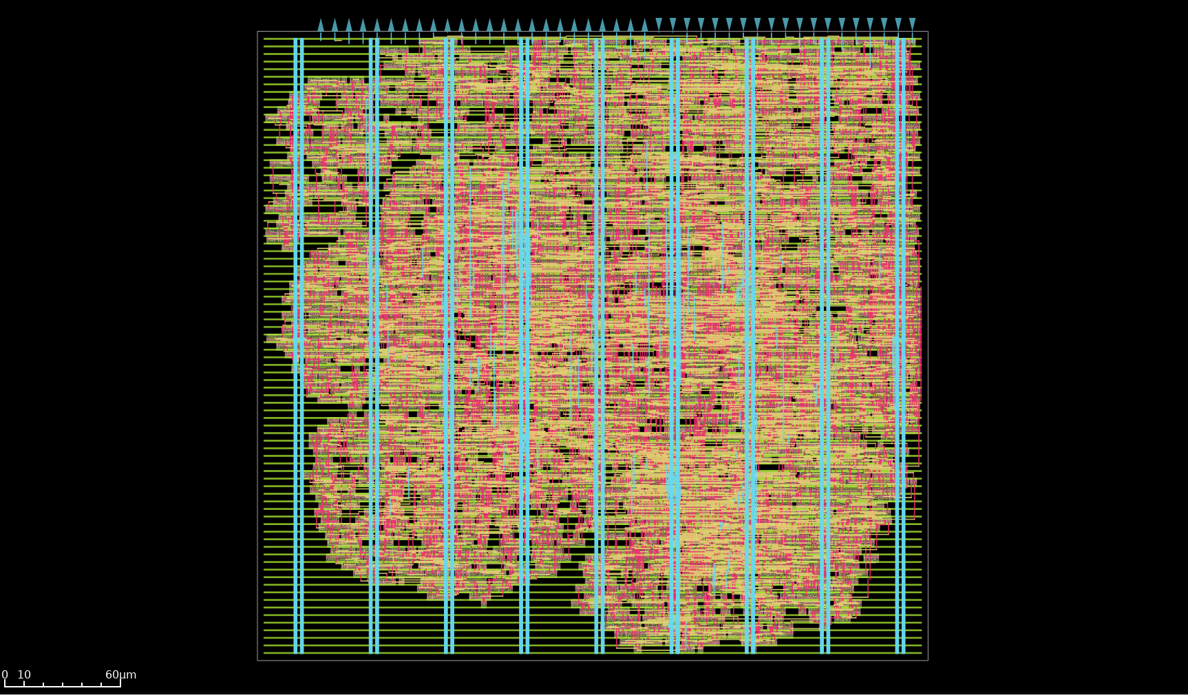
Chronicles of a bad idea. Or how I designed a systolic array with in-silicon debug infrastructure from scratch in under two weeks, and taped it out on Global Foundry 180 nm though a Tiny Tapeout exper